
The Lithography Problem
Lithography now constitutes more than 50% of the cost at advanced semiconductor nodes. EUV, the new lithography technology planned for production in 2019, spans two or more stories in a fab, which must be designed from scratch to accommodate it.
In the GlobalFoundries image at the right, you can see a human operator standing next to a two-story EUV stepper, with a beam source and control room in a separate structure outside the fab.
(click the image to enlarge)
In a recent article in SolidState Technology compares the current 22nm High Volume Manufacturing flow cost breakdowns. The capital expenditure (CapEx) for 8 EUV or 16 ArFi steppers is ~US$1B. The cost of stepper CapEx depreciation per wafer is ~10x the cost of all lithography materials for both ArFi and EUV.
(click the image to enlarge)
Direct-Write Alternatives - Lasers, E-beams and Proton Beams
Various direct-write alternatives have been used in semiconductor manufacturing for many years. Above one micron, lasers (photon beams) could be used, but they wrote slowly. Electron beams are still used to write features in the nanometer range. Today multiple e-beam tools address the mask writing market, but these are still too slow for full wafer high volume manufacturing (HVM).
More recently, another approach has shown promise: directly writing features with proton beams. Protons have many advantages: Their mass is 1800 that of an electron, so fewer protons of a given energy are required to expose the resist. Once a proton beam is collimated, it spreads much less than an electron beam. But nobody has yet been successful collimating protons from a single source into multiple coherent and controllable beams.
The ideal proton beam writer must meet these all of these requirements for HVM:
The Particle source must produce cold protons without much lateral energy, which ultimately produces blur.
The writer must be able to write millions of individually controlled beams simultaneously
The writer must be able to handle the data throughput required to control millions of beams
The beams must be able to write any size features.
Introducing the Transmute ProScan


Transmute started with a simple idea: integrate thousands of proton accelerators onto a silicon chip that could be reproduced easily. Using a separate linear accelerator for each beam guarantees collimation. Building 50nm x 50nm channels on a 100nm pitch to produce a 20nm beam negates the need for reduction optics. The accelerators would have to be 64mm long to achieve an energy of 3.5KeV. 262,000 accelerators in parallel on each chip could write a path one inch wide. Twelve of these print heads with 3 million beams could write a full 300mm wafer fast enough for HVM.
ProScan advantages include:
Direct write - no mask needed
No reduction optics required
Low energy protons are easily colliminated and controlled
Resist is 100 times more sensitive to protons than electrons
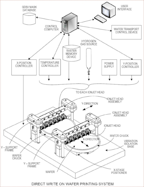
Proscan Architecture
The ProScan system moves the wafer under the print heads at 40cm/s (X direction). Each print station consists of 12 print heads are mounted on a rail that is fixed to the base. A line of pixels (Y direction) is written by all of the print heads. Each print head has nano actuators that can dynamically set its position to adjust for small variations in speed, vibration, and temperature. Just like an inkjet printer, any image can be printed with a minimum feature size of 20nm. ProScan prints all geometries at the same speed with the same minimum feature size and alignment.
A twinscan configuration has two rails of print heads and allows overlap of alignment and exposure. Each print head can sense backscattered electrons to provide information about wafer position and head alignment. Some key points:
The wafer moves at 40cm/sec and the print heads write lines at 2MHz to produce a 20nm pixel.
The linear accelerators are on a 100nm pitch and produce a 20nm beam so the wafer must pass under the print heads five times.
For 300mm wafers, the ProScan system can write 100 wafers/hour regardless of pattern complexity or density.
A ProScan system is similar in size to a 193i scanner.
The data rate is written at 500Gb/sec (62.5GB/s) per head which is supplied by Hybrid Memory Cube (gen.3) technology over 3 twelve channel fiber optic ribbon cables. That is around 6Tb/s per print station.
Project Status

The ProScan system is built using as many standard parts as possible. The footprint is similar to a standard 193i scanner but requires a vacuum. We have explored the initial design and have identified the ion injector as being the critical technology. We are exploring several approaches to reduce the risk. The good news is that positioning and data path technologies have matured in the last few years and the cost and complexity have been greatly reduced.