
Exposure
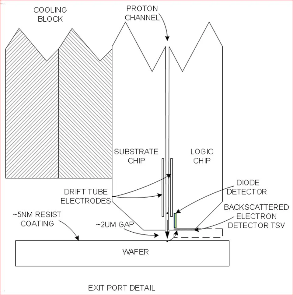
/Accelerator Exit Port
The proton beam exits the accelerator channel and travels across the head to wafer gap to expose the resist on the surface of the wafer. Laser interferometers control the nano actuators on the print head to maintain a two micron distance to the wafer and to keep the head parallel to the surface.
Before a wafer can be exposed, the wafer topology and alignment features must be mapped and stored. Backscatter detectors embedded in the edge of the logic chip sense these features and their position is communicated to the layout controller.

X-Y positioning
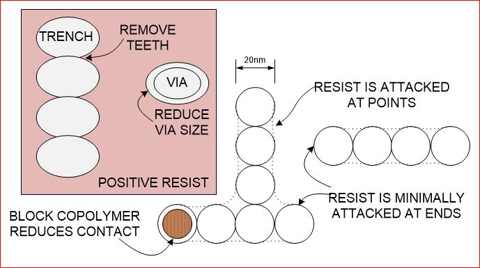
As the wafer travels under the print heads at 40cm/s a line of protons is written across the wafer every 500ns (2MHz) to produce a line of 20nm pixels. Since the pixel is 20nm and the accelerators are on a 100nm pitch, the print heads will shift over by 20nm to paint the next row (X) of pixels. Five passes completely cover the wafer. This shifting of each print head the Y direction is done by the Nano Actuators.
Exposure
PMMA is a popular positive resist used to achieve line widths of 4.4nm (with 50KeV electrons) (jes.ecsdl.org/content/128/1/166). Proton beams are about 100 times more efficient than e-beams. 3.5KeV protons enter the resist moving much slower than the 50KeV electrons. Each electron only produces a few collateral electrons that are moving slow enough to split the polymer bonds. The dissociation energy for a C-C bond is 3.6eV. The electron has to be at rest with respect to the molecule in order to react most strongly via dissociative electron attachment, where the electron comes to rest at the molecule, depositing all its kinetic energy. Protons generate on the order of 100 collateral electrons that are less than 10eV. These not only are effective in splitting the polymer bonds, they also do not spread as much as the hotter electrons from e-beams. Protons can expose PMMA with 7uC/cm2. The write energy and dose are calculated as follows:
7e-6C/cm2 * 3500eV = 0.0245 joules/cm2

7e-6C/cm2 * 6.24e18p/s = 0.437 protons/nm2
0.437 protons/nm2 * 20nm *20nm = 175 protons per pixel
Wafer Heating

The wafer absorbs the proton energy and dissipates it as heat. This will lead to some CD variation across the wafer. We can assume that 99% of the heat will be transferred to the chuck (which is cooled).
wafer area = 3.1416 * ((.3m-.004)/2)^2 = 0.0688m2
wafer heating @ 100% write = 0.0245 joules/cm2 * 10000 cm2/m2 * 0.688m2 = 16.9 joules
wafer heating @ 60% write = 6.74 Joules
wafer temperature rise = 6.74 joules * 0.01 / 37.4 joules/*C = 0.018 *C